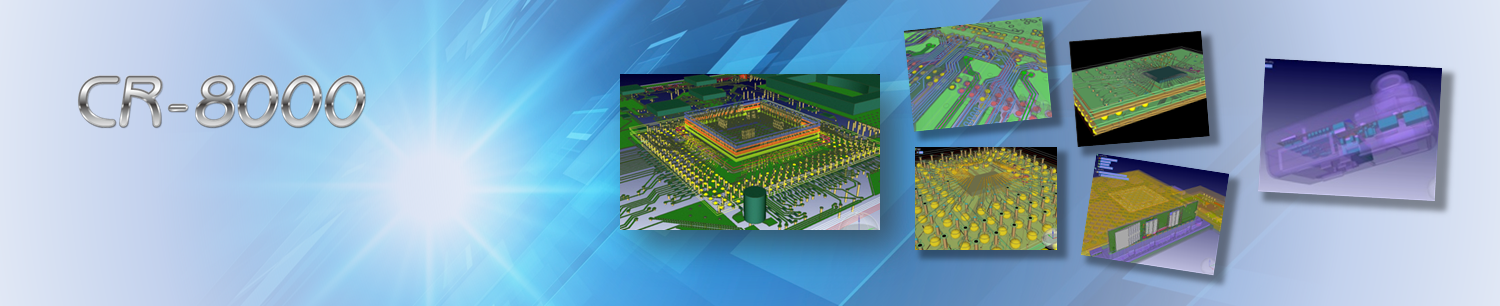
一体化PCB设计桌面
Cadstar是一款具有较高性价比、功能强大的PCB设计解决方案,工作流程直观,在设计过程中很容易指导设计人员。
其集成了单一环境中完成电子开发流程所需的所有技术。
全方位的解决方案包含了示意图、电路板和FPGA系统、PCB布线、高速和信号完整性、EMC分析、3D碰撞分析和生成制造结果。
此外,Cadstar经过了优化,验证了3D环境下的PCB布局。其支持标准3D设计格式(STEP、ACIS、STL和IDF)接口,
可以为电气和机械工程师提供协同设计环境。机械附件中的PCB 3D视图,
使得工程师可以在生成PCB制造结果之前检查冲突和/或所需的间距。
其还配有完整的数据管理功能和广泛的网络访问组件库。尽管功能丰富,但是Cadstar非常经济,
是行政资源有限的个人专业设计师以及小型到中型的设计团队工程师的理想选择。
All-in-One PCB Design Desktop
Cadstar is a powerful PCB design solution of price-performance that allows an intuitive work flow, guiding designers easily
through their design process. It incorporates all the technologies necessary for a complete electronic development process
in a single environment.
The full range of solution includes schematics; board and FPGA-level system, PCB layout, high-speed and signal integrity,
EMC analysis. , 3D collision analysis and creation of manufacturing output. In addition, Cadstar is optimized
for the verification of PCB layouts in 3D environment. Supporting interfaces for standard 3D design format (STEP, ACIS, STL and IDF),
it provides collaborative design environment for electrical and mechanical engineers. The 3D view of the PCB in the mechanical enclosure
allows engineers to check conflicts and/or required spacing before creating manufacturing output of the PCB.
It is also complemented by complete data management capabilities and extensive internet-accessible component libraries.
In spite of its rich features, Cadstar is affordable and fully optimized option even for individual professional designers and
for engineers of small to mid-sized design team with limited administrative resources.
Please just contact us for further information.