CR-8000 Design Gateway
系统级电路设计环境
Design Gateway是支持包括单个PCB板、多个PCB板和PCB板之间的连接在内的整个系统电路的设计/验证的电路设计环境,
在世界上尚无先例。能够以多个PCB板为对象进行分析和设计变更,并依靠高开放性,与IT系统进行高度协作。
随着电子产品小型化、多功能化、高功能化的要求日益强烈,使多个PCB板在复杂协作的同时进行高水平动作的设计不可或缺。
为此,需要高水平设计,以便能够同时设计多个PCB板,并调整相互之间的协作。
Design Gateway提供了系统级电路设计环境,不仅支持单个PCB板的设计,而且还对应包括多个PCB板和连接部分在内的多板概念。
System Level Circuit Design
Design Gateway is the world's first circuit design tool that supports the design and verification of circuits,
including single and multi-board systems and inter-board connections. It provides high level integration with
IT data infrastructures through its open architecture.
Design Gateway provides a system level circuit design environment that supports single board design and multi-board
concepts incorporating boards and connecting parts.
采用了分层和电路块的模块设计
Design Gateway可以将标准化的功能模块作为标准电路块进行库化,可以在利用该模块的电路中,像元器件一样搜索和输入。
此外,电路块还可以设定各种编辑权限,管理电路块的沿用设计。
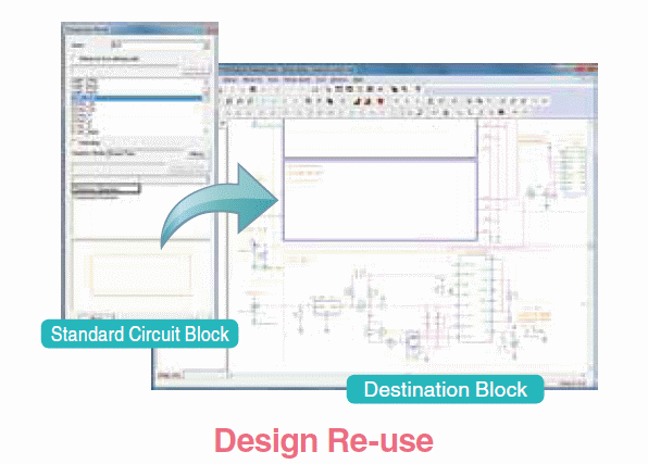
【图像】电路块的沿用设计
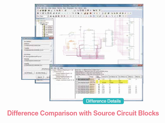
沿用源电路块被更新时,可以按元器件、NET等抽取与沿用电路块的差分。
此外,在沿用目的地电路块上反映沿用源电路块的信息时,为了能够按差分保持沿用目的地的信息,
还能应对希望使沿用目的地电路块的编辑内容优先的情况。
【图像】与沿用源电路块的差分对比
Module Design Using Hierarchical Circuit Blocks
Design Gateway supports the formation of function blocks or modules to be standardized into libraries as
standard circuit blocks. These blocks can be searched and input like component libraries in the circuits
where they are reused.
In addition, a variety of permissions for editing can be set for circuit blocks at their place of reuse,
making possible reuse design using circuit blocks, in accordance with the operation performed.
(Picture) Reuse design with circuit blocks
When original circuit blocks are modified, it is possible to extract the differential of the new circuit block
for each object, such as components and nets.
In addition, when the data for original circuit blocks is reflected in the new circuit block,
the data for the new location can be retained for each differential, allowing users to give preference to edited data
for the new circuit block to be handled.
(Picture) Differential comparison with the original circuit block
通过考虑到电气特性的规则校验来提高电路质量
Design Gateway可以根据元器件和网络中设定的属性,进行各种规则校验。
由于不使用仿真器,因此只需最低限度的必要信息即可进行实用性很高的校验。
通过在网络中设定电压值,可以立即发现疏忽大意导致的设计错误,
比如纳入了元器件的电气特性(常数、额定值)的元器件可靠性校验,元器件反向连接,元器件选择错误导致的额定值不足等。
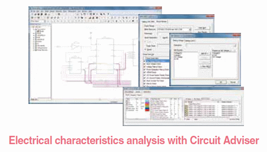
【图像】考虑到电气特性的Circuit Advisor(电路顾问)
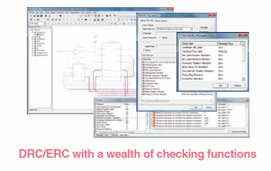
除了考虑到电气特性的校验以外,还可以进行参照的重复、网络名称的重复和接触、电源/地线的短路以及属性的漏填等的校验,
并以错误报告书的形式显示结果。该错误报告书可以与电路图进行交叉搜索,迅速确认错误部位。
【图像】具备丰富校验功能的DRC/ERC
Improved Circuit Quality with Rule Checks Adjusted for Electrical Properties
Design Gateway allows a variety of rule checks, based on the attributes set for components and nets.
Because a simulator is not employed, highly practical checks can be carried out with only the minimum required data.
By setting the voltage for the nets, careless design errors, such as component reliability checks considering component
electric properties (constants, ratings), reversed component connections, insufficient rating due to mistaken component
selection etc. can be instantly discovered.
(Picture) Circuit advisor adjusted for electrical properties
In addition to checks which take electrical properties into account, checks are made for duplicate references,
duplicate net names in whole and in part, power supply and ground short circuits, and missing attribute records,
and the results can be displayed in an error report. This error report allows cross probing with the circuit diagram
so that problem locations can soon be identified.
(Picture) DRC/ERC equipped with a full range of error checking functions
电路设计阶段的预布局SI验证
Design Gateway可以在电路设计初期阶段简单地进行SI分析。 分析工具具备任何人都能简单使用的下列特点:
● 模型设定简便易行(无模型、自动分配)
● 直观并实现半自动化的简便操作面板
● 以适合对比图等分析的形式输出结果
● 追求结果的再利用性(重新显示、加工、文档化)
在设计中途也可以立即分析关键网络,因此消除了在电路完成之后将所有网络都输出到分析系统之类的工具间循环的繁琐性。
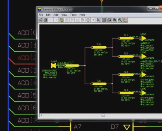
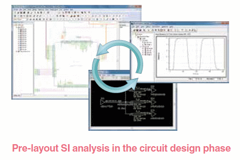
【图像】利用电动编辑器进行预布局SI分析
Pre-Layout SI Verification at the Circuit Design Stage
With Design Gateway, SI analysis can be easily performed from the initial stage of circuit design.
The analysis tools have the following features, which can be easily used by anyone:
*Removal of the need for model setting (model-less, automatic allocation)
*Intuitive semi-automatic operation panel
*Result output in the form of comparison graphs etc. for easy analysis
*Emphasis on reusability of results (redisplay, processing, documentation)
Design Gateway eliminates the effort involved in iteration between tools such as outputting all the nets
to the analysis system after completing a circuit, in order to immediately analyze critical nets during the design phase.
(Picture) Pre-layout SI analysis using the electrical editor
实现与基础设施环境的无缝协作的高开放性
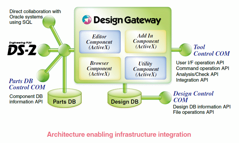
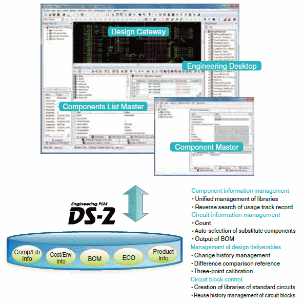
Design Gateway支持Windows的标准API“COM”,具备高开放性,可以与在设计电路时所需的技术信息无缝协作。
不但可以与Engineering PLM DS-2无缝协作,而且还可以与原有系统协作,构建用户特有的设计环境。备有适合协作的界面。
【图像】实现各种基础设施协作的高开放性
利用“DG DS-2 Embedded”,可以在Design Gateway上使用DS-2的功能,并可直接访问用DS-2管理的信息。
・ 元器件主信息的利用
・ PCB板元器件列表的创建与管理
・ 设计数据的管理与利用
【图像】“DG DS-2 Embedded”的概要
Open Architecture
Design Gateway supports COM, which is a Windows' standard API, and provides a highly open architecture for seamless
integration with information accumulated in the infrastructure environments needed when designing circuits.
As well as being seamlessly integrated with our Engineering PLM DS-2, it also integrates with existing infrastructures,
allowing the construction of users’ own design environments. Interfaces for different integration methods are provided.
(Picture) Highly open architecture providing integration with a variety of infrastructures
With DG DS-2 Embedded, DS-2's functions can be used in Design Gateway, allowing direct access to data managed by DS-2.
*Utilization of component master data
*Compilation and management of board parts lists
*Management and utilization of design data
(Picture) Outline of DG DS-2 Embedded
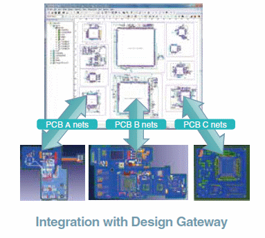
与构思设计/PCB板设计的系统级协作
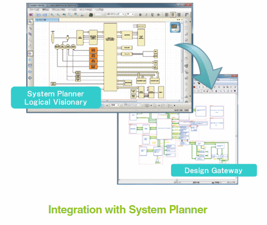
用构思设计环境“System Planner”创建的系统图,可以直接作为Design Gateway的系统电路读入。
此外,还可以根据系统电路的网表信息,用多板设计环境“Design Force”在连接多PCB板的状态下进行多板布局设计。
因此,在构思设计/电路设计/PCB板设计方面,实现了系统级的紧密协作。
【图像】从System Planner的构思设计信息读入到Design Gateway的系统电路图中
【图像】从Design Gateway的系统电路图将多个PCB板的布局输出到Design Force上
Seamless flow as a System from Upfront Design Planning to Board Design
System diagrams planning created with System Planner, our system level design tool,
can be incorporated unmodified as Design Gateway system circuits.
In addition, net list data compatible with multiple boards can be compiled from system circuits,
and multi-board layout design can be performed as connected in Design Force, our system level multi-board design tool.
In this way, Design Gateway provides tight integration at a system level for conceptual design,
circuit design and board design.
(Picture) Incorporation into a system circuit diagram in Design Gateway from design planning data in System Planner
(Picture) Output of multiple board layouts from a system circuit diagram in Design Gateway to Design Force
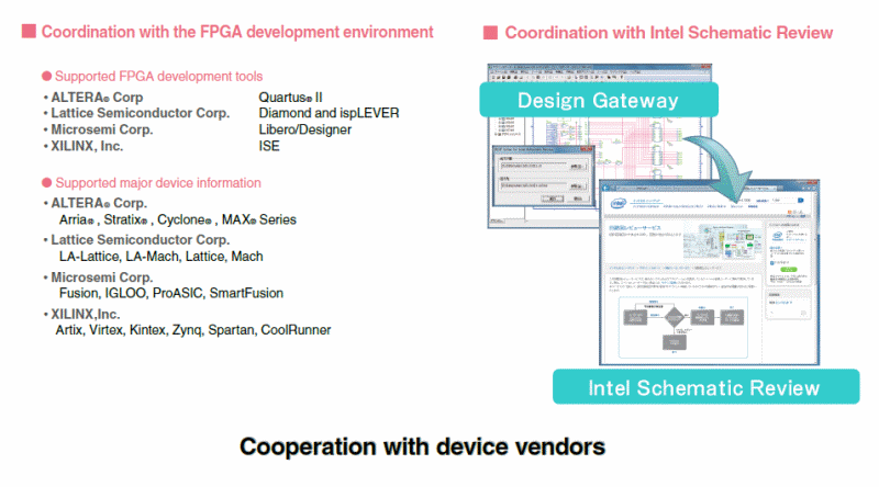
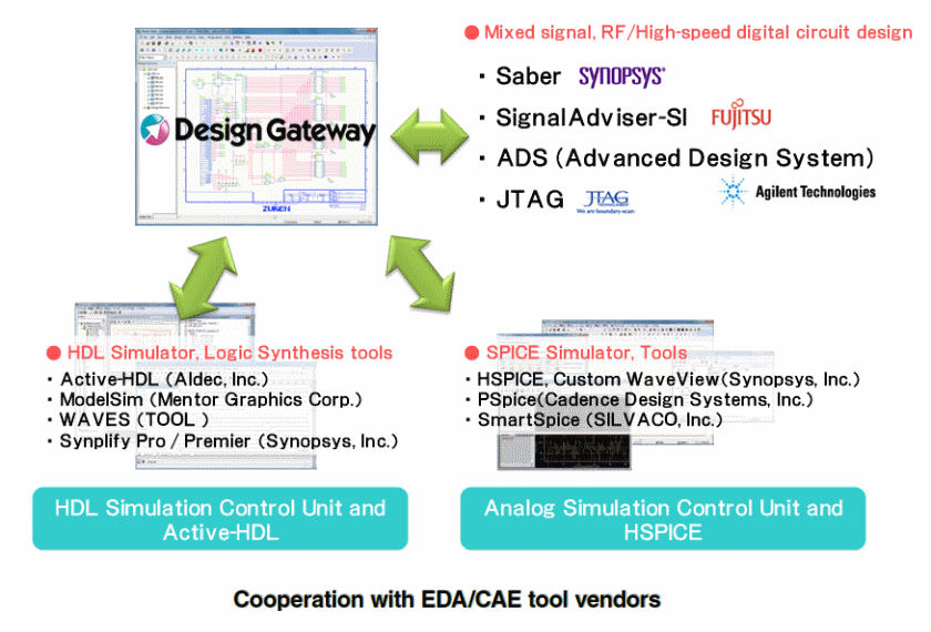
与设备供应商和EDA/CAE工具供应商的协调
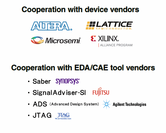
为了支持使用了FPGA/CPLD、插件专用微处理器的设计,本公司也力求与装置供应商密切合作。
与PCB-FPGA协同设计环境“GPM”协作,支持装置供应商提供的FPGA开发工具、设计工具包。
关于协调装置供应商
为了支持难度日益加大的电子装置设计,本公司也力求与第三方供应商的设计工具密切协作,
以便强有力地支持整个电路设计/验证环境。
关于协调EDA/CAE工具供应商
Collaboration with Device Vendors and EDA/CAE Tool Vendors
Zuken is working to maintain close collaboration with device vendors. Integrated with GPM,
our PCB-FPGA co-design environment, Design Gateway supports design kits and FPGA development tools
provided by device vendors.
Collaborating device vendors
Design Gateway provides strong overall backup for circuit design and verification environments through tight integration
with third party design tools, in order to support the increasingly difficult task of designing electronic devices.
Collaborative EDA/CAE tool vendors